Custom-designed and 3D-nanoprinted down-tapered fibers on JLT front cover
In their recent publication in IEEE/OSA’s Journal of Lightwave Technology, B-PHOT researchers proposed a new fiber-to-chip coupling strategy, making use of 3D-nanoprinted down-tapered fibers. A graphical illustration of their novel connectivity concept has been chosen to be depicted on the Journal’s front cover.
Much alike electronic components that are being integrated into a single chip, called an integrated circuit, optical systems and devices are nowadays also being integrated into photonic integrated circuits (PIC) or chips. Whereas these small-sized components offer the potential for reduced space requirements, the optical coupling from and to these chips is often very challenging, because the waveguides on a PIC typically have (sub-)micrometer sizes and are therefore an order of magnitude smaller than the core of a typical optical fiber.
Connections between standard single-mode fibers and waveguides in photonic integrated circuits tend to have relatively high coupling losses due to a difference in mode size between both light guiding media. An accurate interface between both is therefore key for the practical use of such chips. Consequently, the fiber tips and on-chip waveguides are usually adapted to accommodate the dimensional conversion needed to achieve low coupling losses.
Edge coupling strategies involving specialty fibers are frequently used to obtain the best performance in terms of coupling efficiency, bandwidth and polarization independence. Among the different types of specialty fibers, lensed fibers are commonly used to reduce the mode size from the optical fiber towards the on-chip waveguides. With this free-space coupling approach however, Fresnel reflections at the optical interfaces can reduce the coupling efficiency, and robust packaging with epoxies and gels becomes very difficult.
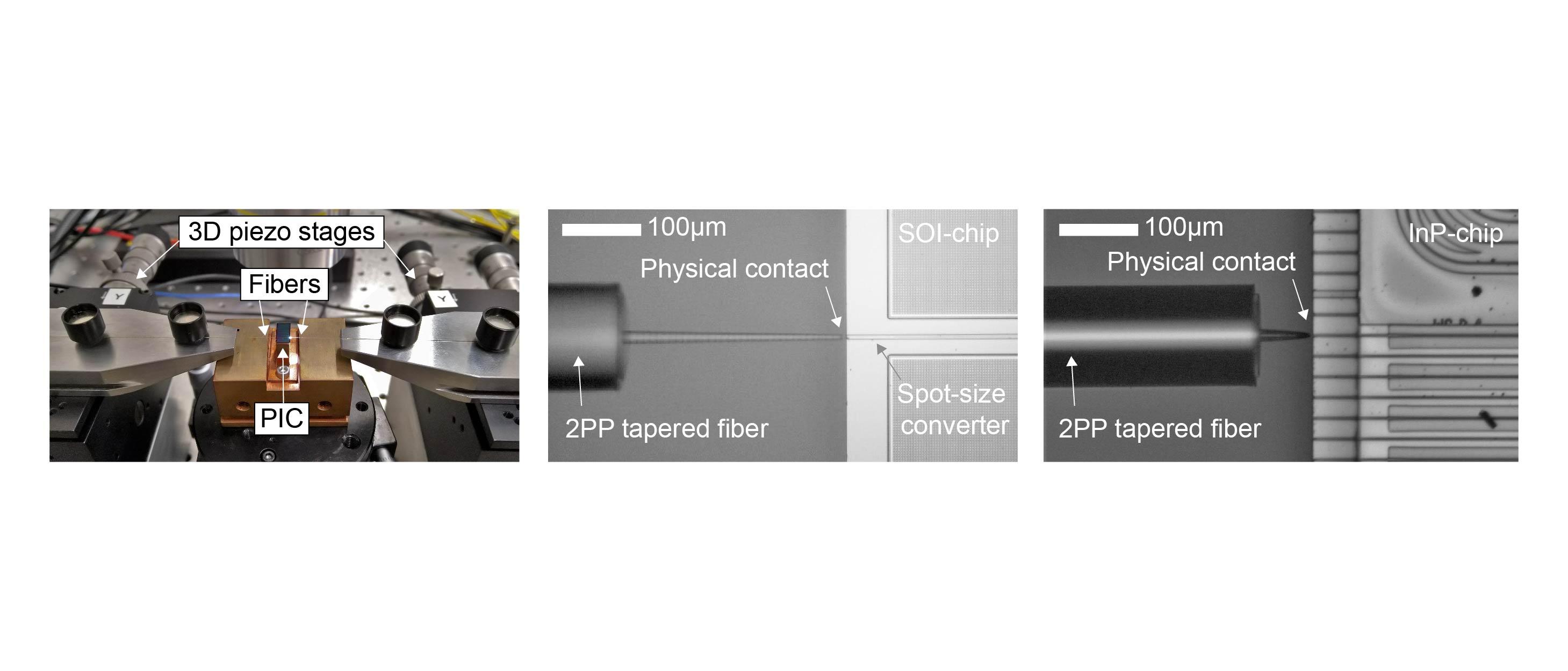
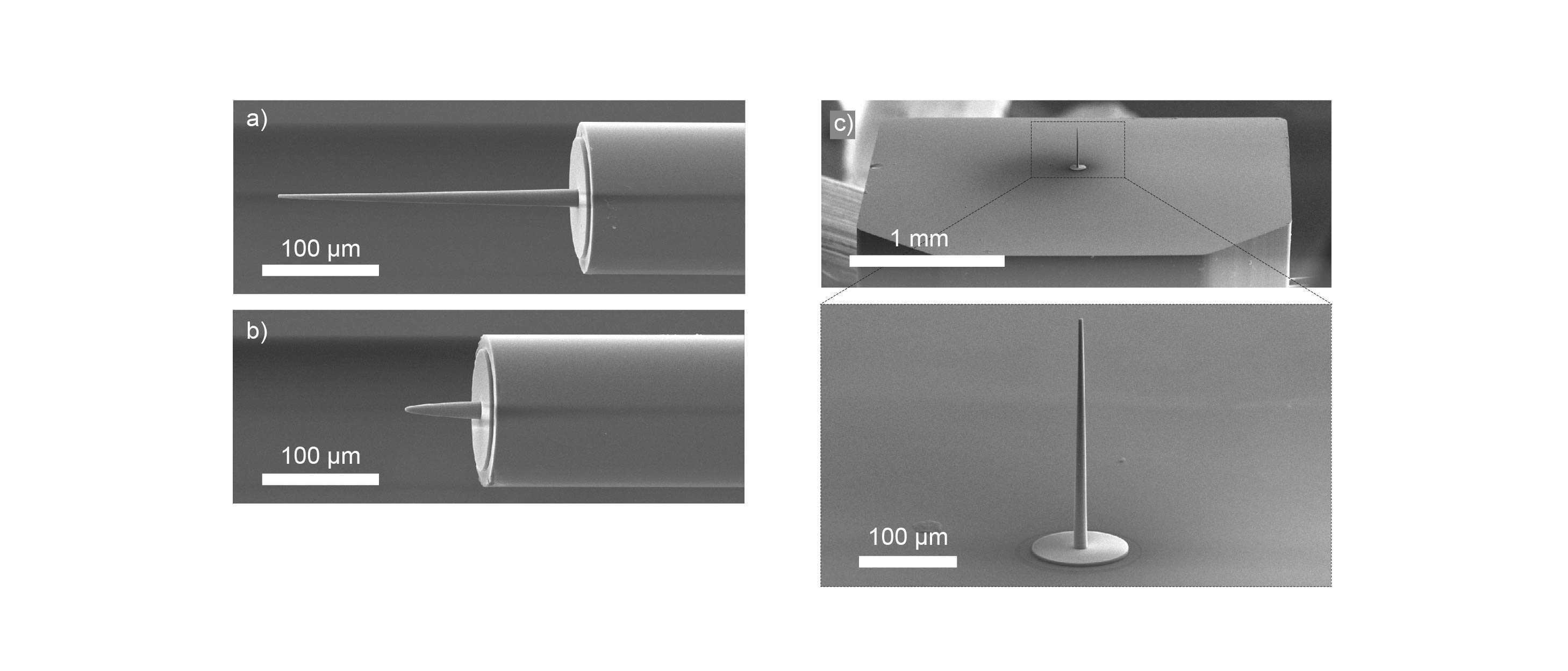
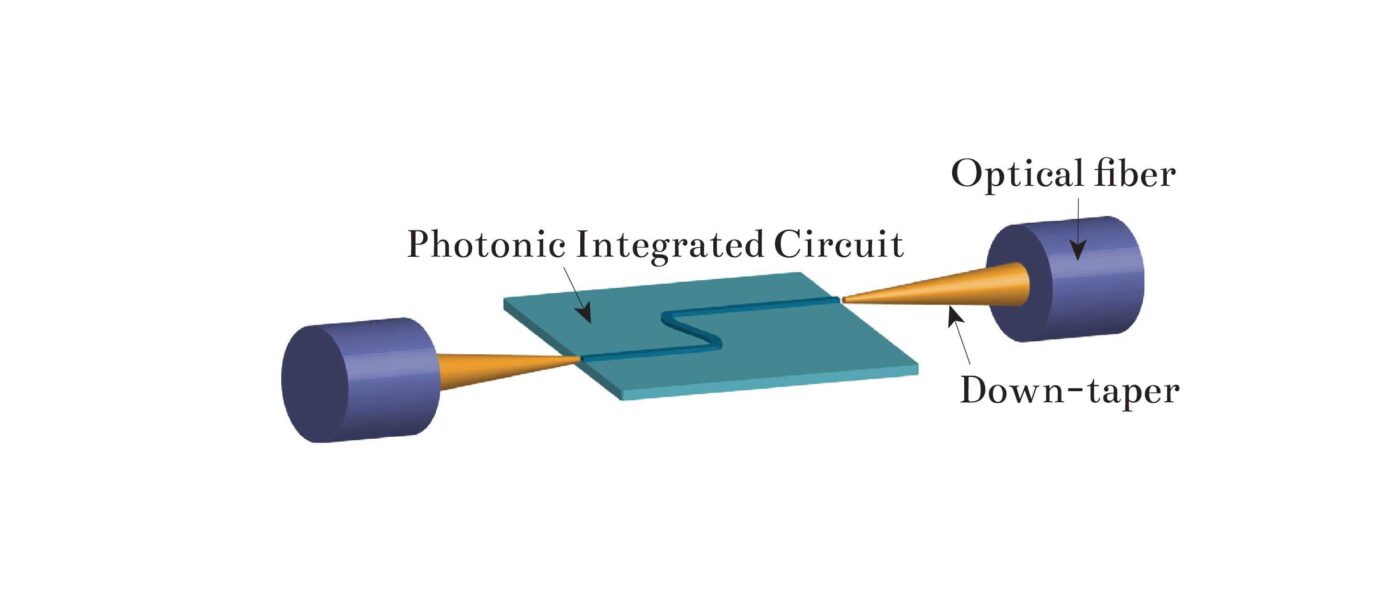
To overcome the above challenges, Dr. Koen Vanmol and his B-PHOT colleagues proposed a novel coupling strategy enabled by the 2-photon polymerization (2PP)-based 3D nanoprinting technology, allowing to print down-taper structures directly on standard telecom optical fibers tips to reduce their mode sizes. The 2PP technology enables the required design flexibility and fabrication resolution to tailor the taper’s design to precisely match the on-chip waveguide’s mode-fields. Moreover, these custom down-tapered fibers allow for physical contact between the on-chip waveguides and fibers in order to reduce Fresnel reflections and increase the potential for robust packaging.
The paper discusses the design and optimization of the down-taper’s geometry, after which they are directly printed on the cleaved end-facet of standard telecom single-mode optical fibers. The fabricated specialty fibers are finally characterized for their output modal fields and their fiber-to-chip coupling performance is demonstrated with 5 generic PIC platforms, making use of 3 different material platforms, namely silicon-on-insulator, silicon nitride and indium phosphide chips. The results are compared with commercially available lensed fibers, showing that B-PHOT’s 2PP down-tapered fibers achieve equal or better coupling efficiency for 4 out of the 5 investigated PIC platforms, with a measured improvement in coupling efficiency up to 1.43 dB.
With the obtained promising results, the concept of 2PP down-tapered fibers can remove the restrictions on PIC waveguides to match the specifications of the available specialty fibers, and can therefore potentially save valuable chip real estate. In addition, the mode-matched physical contact coupling strategy can potentially facilitate the widespread adoption of PICs in industry and research. Additional work on the development of 2PP tapered fibers can be found in the following recent publication: 10.1364/OE.409148.
Mode-field Matching Down-Tapers on Single-Mode Optical Fibers for Edge Coupling Towards Generic Photonic Integrated Circuit Platforms